Quick Start
This guide introduces the FoBE Breakout CMSIS-DAP Lite and how to use it.
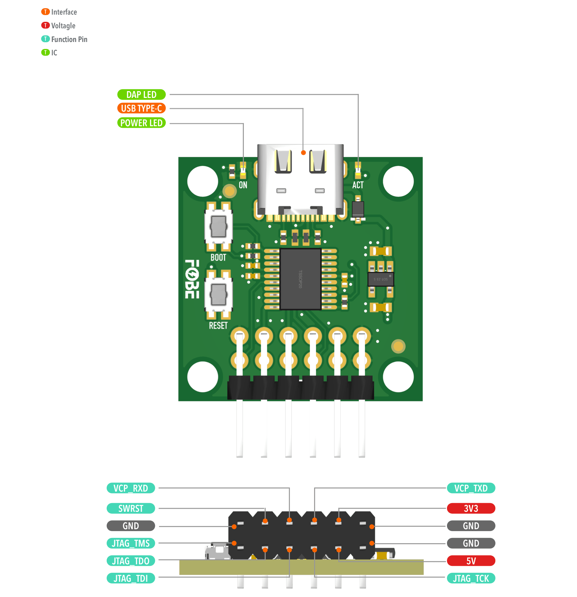
Hardware diagram
The following figure illustrates the FoBE Breakout CMSIS-DAP Lite hardware diagram.
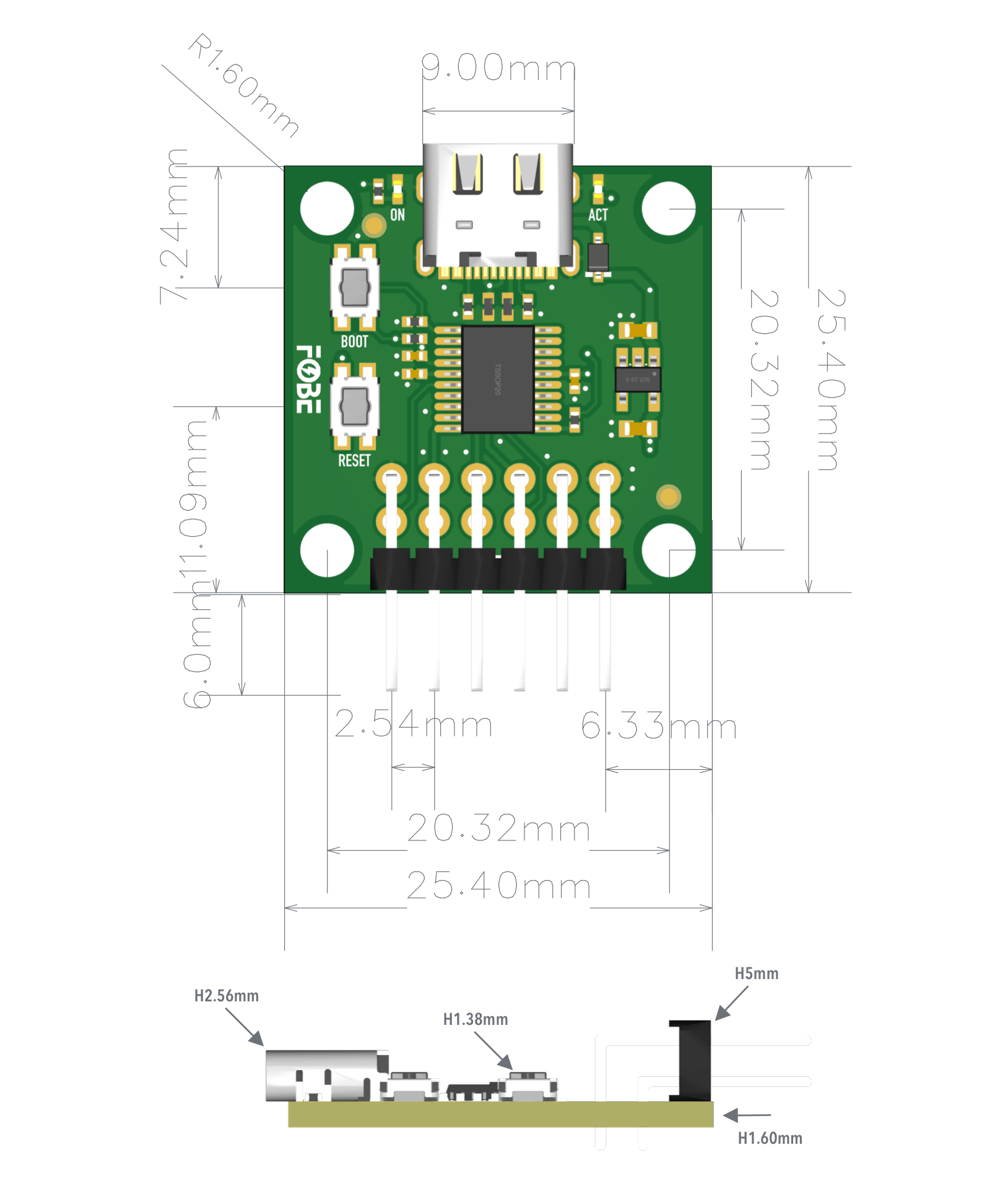
Mechanical dimensions
FoBE Breakout CMSIS-DAP Lite is a single-sided 25.4mm x 25.4mm (1" x 1") 1.6mm thick PCB with a USB-C connector and a set of 12-pin 2.54mm header. Features two buttons for reset and bootloader mode, and a DAP-LED for status indication. Fixing by 4 x 1.6mm Screw holes.
Interfaces
The module provides a 12-pin 2.54mm header interface for connection to target boards.
| Pin | Signal | Features |
|---|---|---|
| 1 | VCP_RXD | Virtual COM Port Receive (RX) |
| 2 | VCP_TXD | Virtual COM Port Transmit (TX) |
| 3 | 3V3 | Power output: 3.3V |
| 4 | 5V | Power output: 5V |
| 5 | GND | Ground |
| 6 | SWRST | Software Reset |
| 7 | JTAG_TMS | JTAG Test Mode Select |
| 8 | JTAG_TDO | JTAG Test Data Output |
| 9 | JTAG_TDI | JTAG Test Data Input |
| 10 | JTAG_TCK | JTAG Test Clock |
| 11 | — | Reserved |
| 12 | — | Reserved |
Usage Example
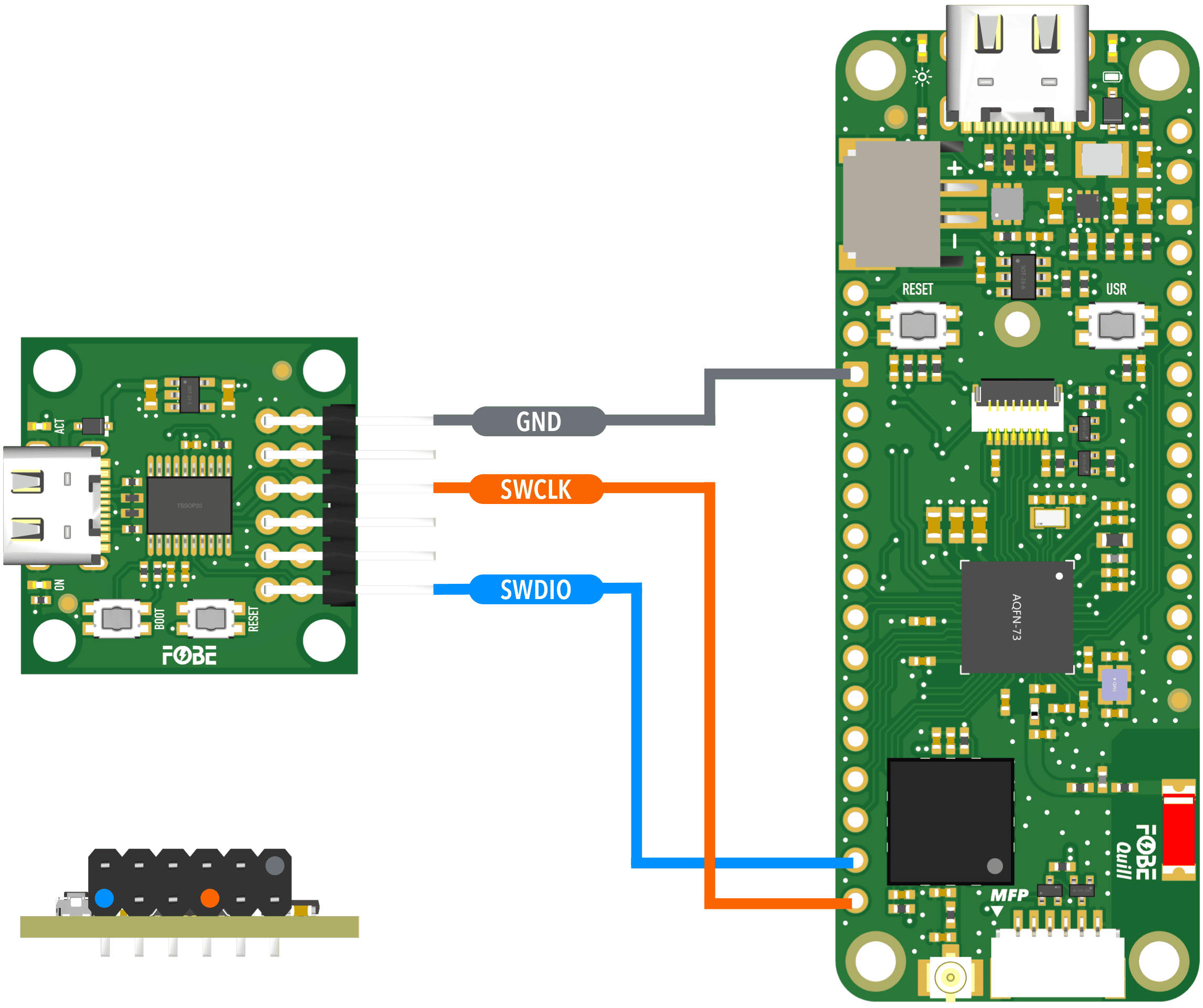
Connection with FoBE Quill nRF52840 Mesh
Connect the FoBE Breakout CMSIS-DAP Lite to the FoBE Quill nRF52840 Mesh using the provided Dupont wires.
Setup Instructions
-
Hardware Connection
- Connect the CMSIS-DAP Lite to your target board using the 12-pin header
- Ensure proper power supply connections (3.3V or 5V as required)
- Connect SWD signals: SWCLK, SWDIO, and SWRST
- Connect USB-C cable to your development computer
-
Software Setup
- Install your preferred IDE (Keil MDK, IAR, or OpenOCD)
- Configure the debugger to use CMSIS-DAP interface
- Select the appropriate target device in your IDE
- Start debugging or programming your target device
-
Status Indicators
- DAP-LED indicates the current operation status
- Use RESET button to reset the target device
- Use BOOT button to enter bootloader mode for firmware updates
note
- Ensure proper power supply compatibility between the debugger and target board
- Use appropriate voltage levels (3.3V or 5V) for your target device
- The virtual serial port can be used for debugging output and communication