Quick Start
This guide introduces the FoBE Breakout GP8303 and how to use it.
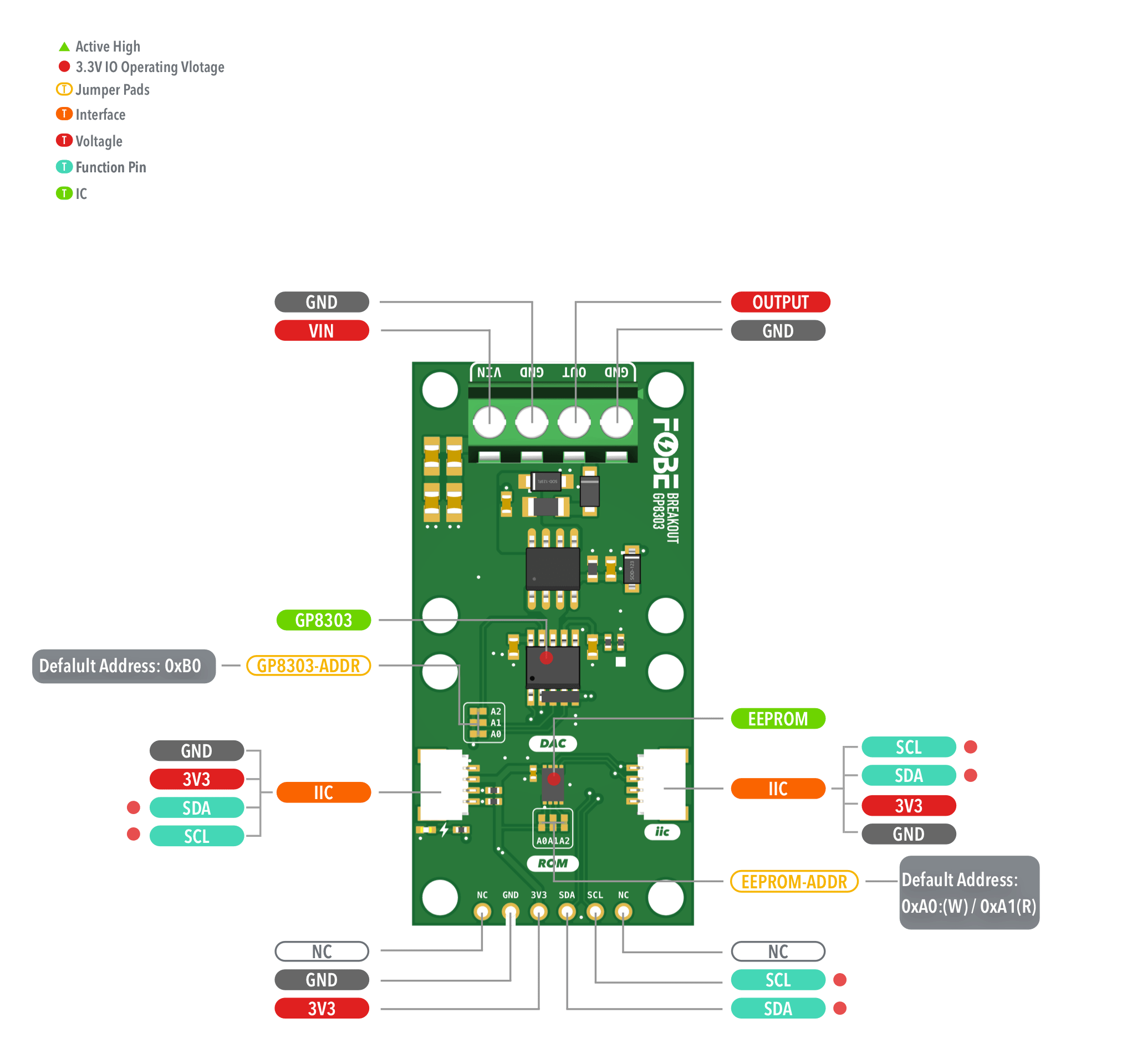
Hardware diagram
The following figure illustrates the FoBE Breakout GP8303 hardware diagram.
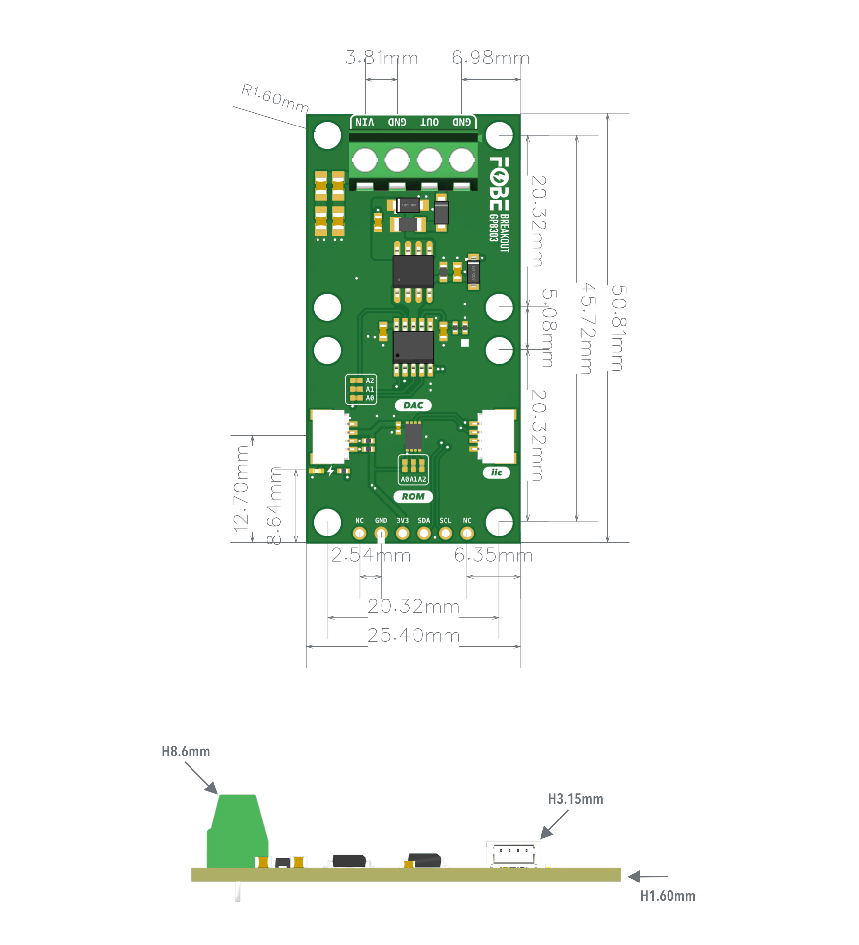
Mechanical dimensions
FoBE Breakout GP8303 is a single-sided 25.4mm x 50.8mm (1" x 2") 1.6mm thick PCB with two SH1.0 4-pin connectors, a set of 6-pin 2.54mm header holes, and 4 x 3.81mm screw terminal blocks for output. Fixing by 4 x 1.6mm Screw holes.
Interfaces
The module provides dual 4-Pin JST SH1.0 connectors, compatible with STEMMA QT / Qwiic.
| 2.54mm 6-Pin | JST-SH1.0 | Features |
|---|---|---|
| NC | — | Not connected |
| GND | GND | Ground |
| 3V3 | 3V3 | Power supply, Only 3.3V |
| SDA | SDA | I2C-Data line |
| SCL | SCL | I2C-Clock line |
| NC | — | Not connected |
Output Terminal Block
| 3.81mm Terminal | Features |
|---|---|
| VIN | Power supply: 18V to 36V |
| GND | Ground |
| OUTPUT | Analog current output: 4-20mA |
| GND | Ground |
Advanced
Address Selection
GP8303 I2C Address
The GP8303 I²C address can be configured using solder pads A0-A2:
| A2 | A1 | A0 | I²C Address |
|---|---|---|---|
| 0 | 0 | 0 | 0x58 (Default) |
| 0 | 0 | 1 | 0x59 |
| 0 | 1 | 0 | 0x5A |
| 0 | 1 | 1 | 0x5B |
| 1 | 0 | 0 | 0x5C |
| 1 | 0 | 1 | 0x5D |
| 1 | 1 | 0 | 0x5E |
| 1 | 1 | 1 | 0x5F |
EEPROM I2C Address
The M24C64 EEPROM I²C address can be configured using solder pads A0-A2:
| A2 | A1 | A0 | I²C Address |
|---|---|---|---|
| 0 | 0 | 0 | 0x50 (Default) |
| 0 | 0 | 1 | 0x51 |
| 0 | 1 | 0 | 0x52 |
| 0 | 1 | 1 | 0x53 |
| 1 | 0 | 0 | 0x54 |
| 1 | 0 | 1 | 0x55 |
| 1 | 1 | 0 | 0x56 |
| 1 | 1 | 1 | 0x57 |
Programming
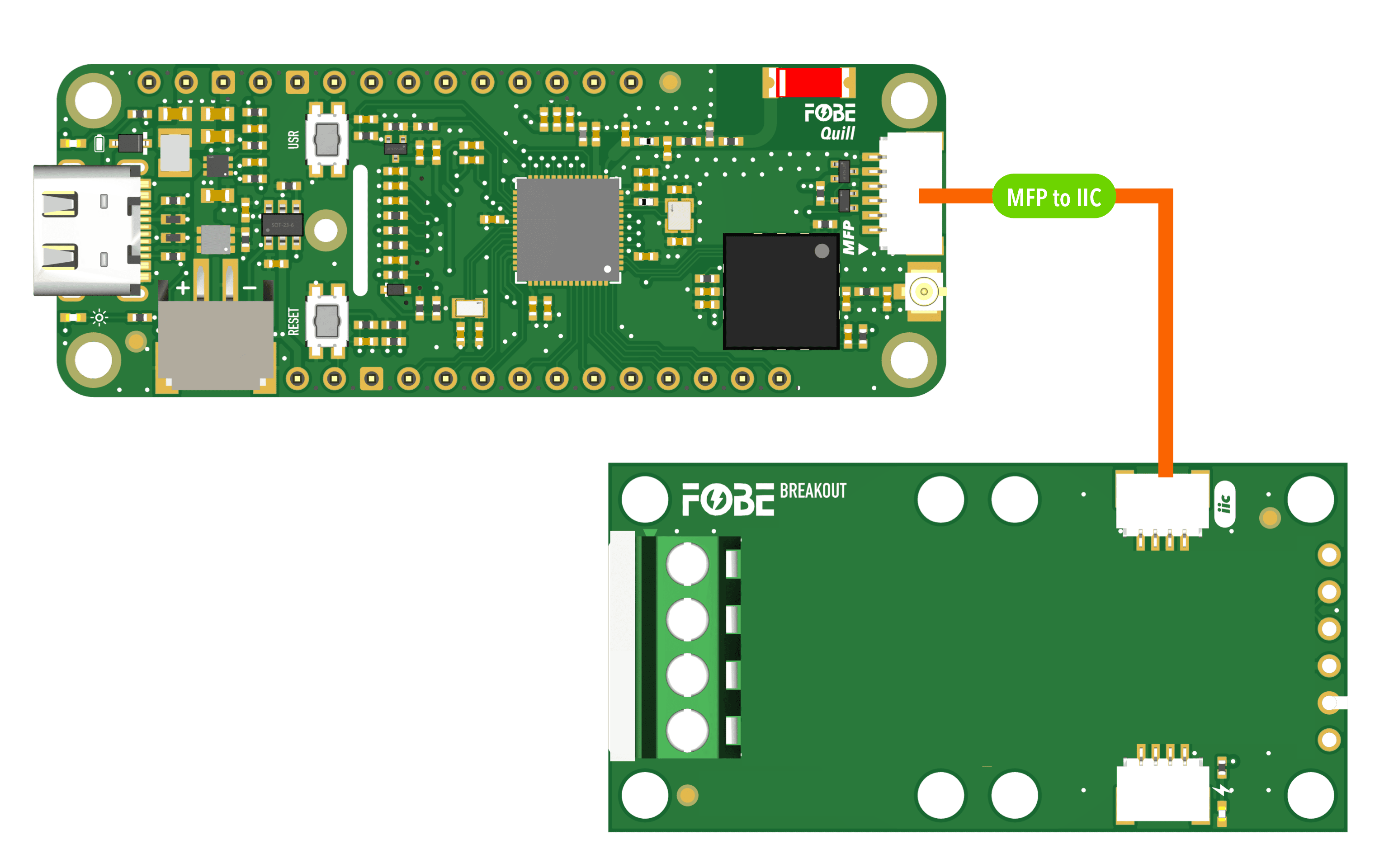
Running with FoBE Quill ESP32S3 Mesh
Let's get started with the FoBE Quill ESP32S3 Mesh using the MFP interface.
- Connect the FoBE Breakout GP8303 to the FoBE Quill ESP32S3 Mesh using the MFP interface.
-
Create a sketch or PlatformIO project, or follow the FoBE Quill ESP32S3 Programming Guide for pre-configuration.
-
Copy the following code into your sketch or PlatformIO project:
#include <Arduino.h>
#include <Wire.h>

// GP8303 I2C Address and Registers
#define GP8303_ADDR 0x58
#define REG_DAC_DATA   0x02    // DAC data register

#define IIC_SDA_PIN    PIN_MFP3
#define IIC_SCL_PIN    PIN_MFP4

bool setDACCurrent(uint8_t address, uint16_t cur_levl) {
    uint8_t hibyte = ((cur_levl << 4) & 0xff00) >> 8;
    uint8_t lobyte = ((cur_levl << 4) & 0xff);
    cur_levl = lobyte << 8 | hibyte;
    Wire.beginTransmission(address);
    Wire.write((uint8_t)REG_DAC_DATA);
    Wire.write((uint8_t)(cur_levl >> 8));
    Wire.write((uint8_t)(cur_levl & 0xFF));
    return (Wire.endTransmission() == 0);
}

void setup() {
  Serial.begin(115200);

  pinMode(PIN_PERI_EN, OUTPUT);
  digitalWrite(PIN_PERI_EN, HIGH);   // Enable peripheral power

  Wire.begin(IIC_SDA_PIN, IIC_SCL_PIN);

  Wire.beginTransmission(GP8303_ADDR);
  if (Wire.endTransmission() == 0) {
      Serial.println("GP8303 DAC found.");
  } else {
      Serial.println("GP8303 DAC not found. Check connections.");
      while (1) delay(1000);
  }

  // set output current of 0-20ma(0-4095)
  setDACCurrent(GP8303_ADDR, 1024);
  Serial.println("DAC current set to 1024 (approx. 5mA).");
}

void loop() {
  delay(1000);
}
This example code sets the DAC output to 16mA. Make sure to connect an appropriate power supply (18V-36V) to the VIN terminal and connect your measurement equipment to the OUTPUT terminal.
# platformio.ini
[env:fobe_quill_esp32s3_mesh]
platform = FoBE Espressif 32
board = fobe_quill_esp32s3_mesh
framework = arduino
monitor_speed = 115200
monitor_raw = true
- Build and upload the project. You should measure 16mA output on the output terminal.
GP8303 DAC found.
DAC current set to 1024 (approx. 5mA).
- If you want to use custom pins, you can change the
IIC_SDA_PINandIIC_SCL_PINdefinitions to your desired GPIO pins. - The GP8303 I²C address can be changed by soldering the appropriate address jumper pads on the board.
- Ensure proper 18V-36V power supply connection to VIN terminal for correct current output operation.