Quick Start
This guide introduces the FoBE Breakout AS5600 and how to use it.
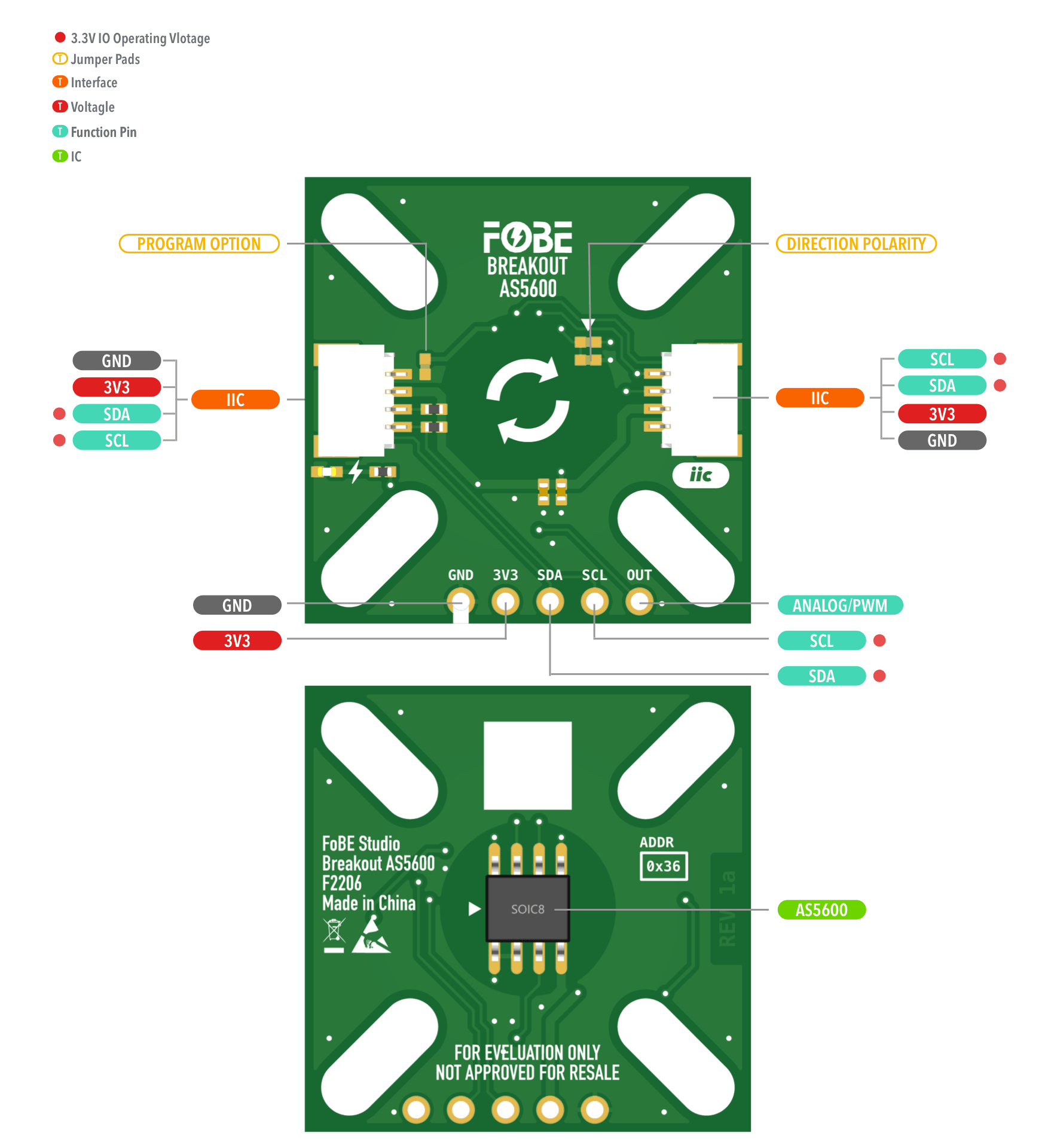
Hardware diagram
The following figure illustrates the FoBE Breakout AS5600 hardware diagram.
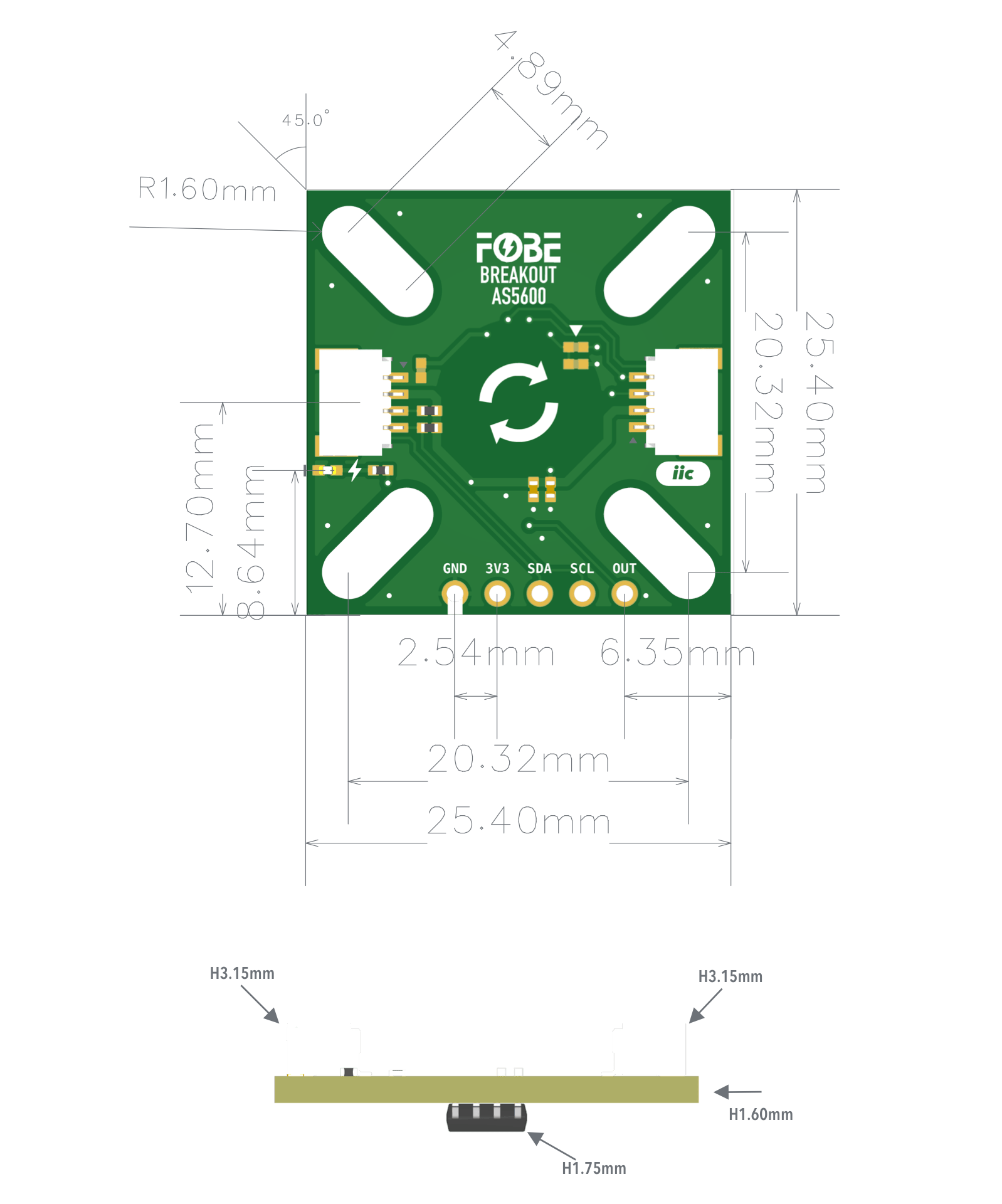
Mechanical dimensions
FoBE Breakout AS5600 is a single-sided 25.4mm x 25.4mm (1" x 1") 1.6mm thick PCB with two SH1.0 4-pin connectors and a set of 5-pin 2.54mm header holes. Fixing by 4 x 1.6mm Screw holes.
Interfaces
The module provides dual 5-Pin JST SH1.0 connectors, compatible with STEMMA QT / Qwiic.
| 2.54mm 5-Pin | JST-SH1.0 | Features |
|---|---|---|
| GND | GND | Ground |
| 3V3 | 3V3 | Power supply, Only 3.3V |
| SDA | SDA | I2C-Data line |
| SCL | SCL | I2C-Clock line |
| OUT | — | Analog/PWM output |
Advanced
Jumper
The module features two jumper pads:
| Interface | Description |
|---|---|
| PROGRAM OPTION | Angle programming mode selector: Connected: Programming via OUT pin Disconnected: Programming via I²C interface (Default) |
| DIRECTION POLARITY | Direction polarity selector: Lower position: Values increase clockwise Upper position: Values increase counterclockwise |
Programming
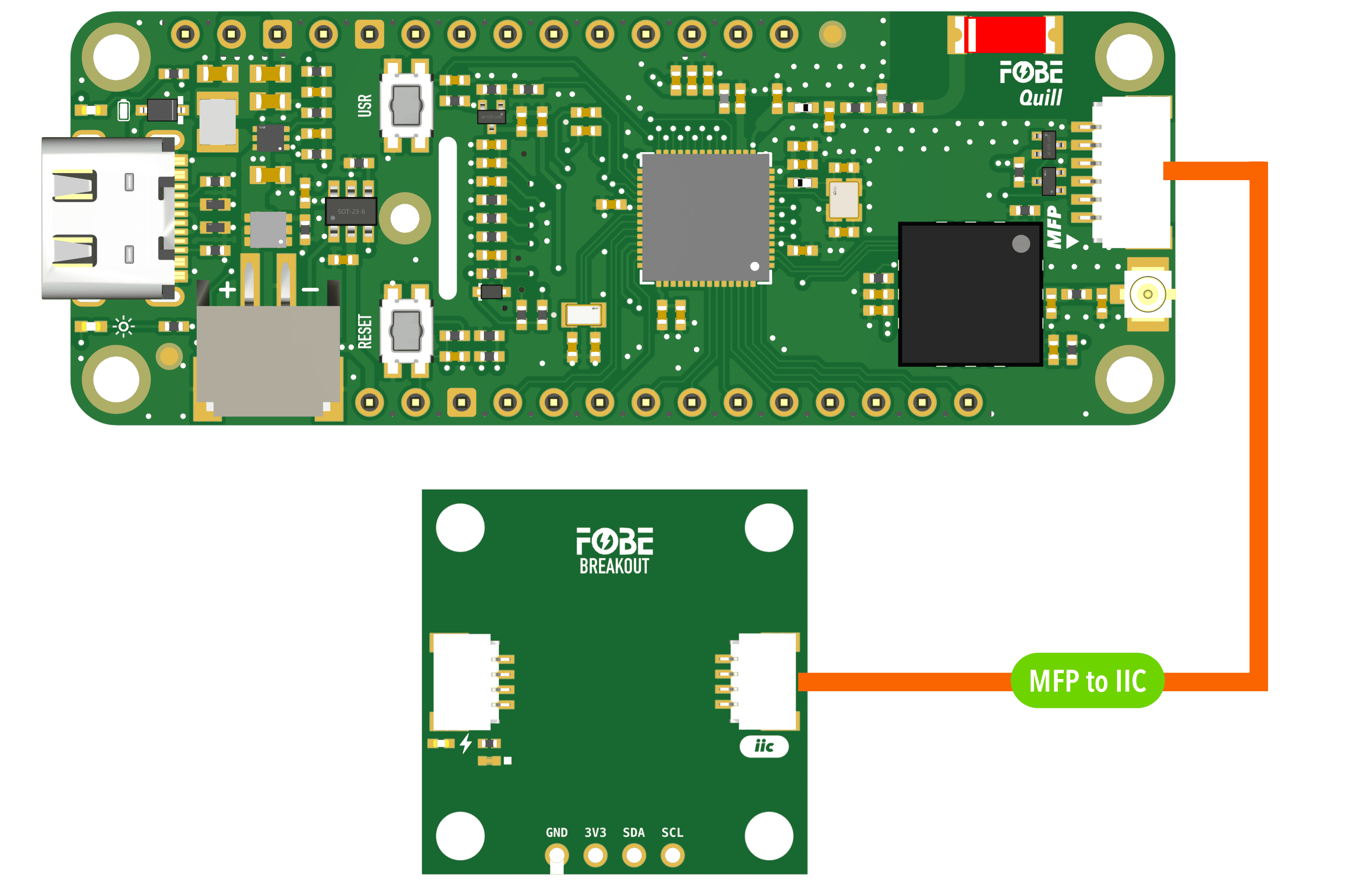
Running with FoBE Quill ESP32S3 Mesh
Let's get started with the FoBE Quill ESP32S3 Mesh using the MFP interface.
- Connect the FoBE Breakout AS5600 to the FoBE Quill ESP32S3 Mesh using the MFP interface.
-
Create a sketch or PlatformIO project, or follow the FoBE Quill ESP32S3 Programming Guide for pre-configuration.
-
Install the necessary library in your project:
robtillaart/AS5600@^0.6.6
- Copy the following code into your sketch or PlatformIO project:
#include <Arduino.h>
#include "AS5600.h"

#define I2C_ADDRESS 0x36        // I2C address definition for AS5600L
#define I2C_SDA_PIN PIN_MFP3    // SDA pin for MFP to I2C cable, change if needed
#define I2C_SCL_PIN PIN_MFP4    // SCL pin for MFP to I2C cable, change if needed
#define PERI_EN_PIN PIN_PERI_EN // Peripheral enable pin, change if needed

AS5600L sensor;

// Variables for speed calculation
float lastAngle = 0.0;
unsigned long lastTime = 0;
float angularVelocity = 0.0;

void setup()
{
  // Initialize serial communication
  Serial.begin(115200);
  Serial.println("Serial initialized");

  // Initialize peripheral power
  if (PERI_EN_PIN >= 0)
  {
    pinMode(PERI_EN_PIN, OUTPUT);
    digitalWrite(PERI_EN_PIN, HIGH); // Enable peripheral power
    Serial.println("Peripheral power enabled");
  }

  // Initialize sensor
  Wire.begin(I2C_SDA_PIN, I2C_SCL_PIN);
  sensor.begin(4);
  Serial.println("I2C bus initialized");

  // Configure sensor first
  sensor.setDirection(AS5600_CLOCK_WISE);
  sensor.setAddress(I2C_ADDRESS);

  while (!sensor.isConnected())
  {
    delay(200);
  }
  Serial.println("AS5600L sensor initialized");

  // Initialize timing for speed calculation
  lastTime = millis();
}


void loop()
{
  delay(50); // Wait equivalent to sensor.wait()

  // Equivalent to sensor.update() == RESULT_OK
  if (sensor.isConnected())
  {
    unsigned long currentTime = millis();
    uint16_t angle = sensor.readAngle();
    float degrees = sensor.rawAngle() * AS5600_RAW_TO_DEGREES;

    // Calculate angular velocity (degrees per second)
    float deltaTime = (currentTime - lastTime) / 1000.0; // Convert to seconds
    float deltaAngle = degrees - lastAngle;

    // Handle angle wraparound (0-360 degrees)
    if (deltaAngle > 180.0) {
      deltaAngle -= 360.0;
    } else if (deltaAngle < -180.0) {
      deltaAngle += 360.0;
    }

    if (deltaTime > 0) {
      angularVelocity = deltaAngle / deltaTime;
    }

    // Update last values
    lastAngle = degrees;
    lastTime = currentTime;

    // Get additional sensor parameters
    uint16_t magnitude = sensor.readMagnitude();
    uint8_t status = sensor.readStatus();
    uint8_t agc = sensor.readAGC();

    // Always display data (remove the condition check that was blocking output)
    // Display data on screen
    Serial.print("\033[H\033[J");
    Serial.println("> FoBE Breakout AS5600 Monitor");
    Serial.println();
    Serial.print("\033[7m");
    Serial.printf("%-12s%-12s%-12s\n", "INDEX", "VALUE", "UNIT");
    Serial.print("\033[0m");
    Serial.printf("%-12s%-12d%-12s\n", "ANGLE", angle, "RAW");
    Serial.printf("%-12s%-12.2f%-12s\n", "DEGREES", degrees, "°");
    Serial.printf("%-12s%-12.2f%-12s\n", "VELOCITY", angularVelocity, "°/s");
    Serial.printf("%-12s%-12d%-12s\n", "MAGNITUDE", magnitude, "");
    Serial.printf("%-12s%-12d%-12s\n", "STATUS", status, "");
    Serial.printf("%-12s%-12d%-12s\n", "AGC", agc, "");
  }
}
This example code uses ANSI output formatting. Your terminal must support ANSI escape codes to display the output correctly.
# platformio.ini
[env:fobe_quill_esp32s3_mesh]
platform = FoBE Espressif 32
board = fobe_quill_esp32s3_mesh
framework = arduino
lib_deps =
	robtillaart/AS5600@^0.6.6
monitor_speed = 115200
monitor_raw = true
- Build and upload the project. You should see the FoBE Breakout AS5600 Monitor output in the serial monitor (raw mode).
> FoBE Breakout AS5600 Monitor

INDEX       VALUE       UNIT
ANGLE       2665        RAW
DEGREES     234.23      °
VELOCITY    0.00        °/s
MAGNITUDE   1122
STATUS      51
AGC         128