Quick Start
This guide introduces the FoBE Breakout OLED 0.42 inch and how to use it.
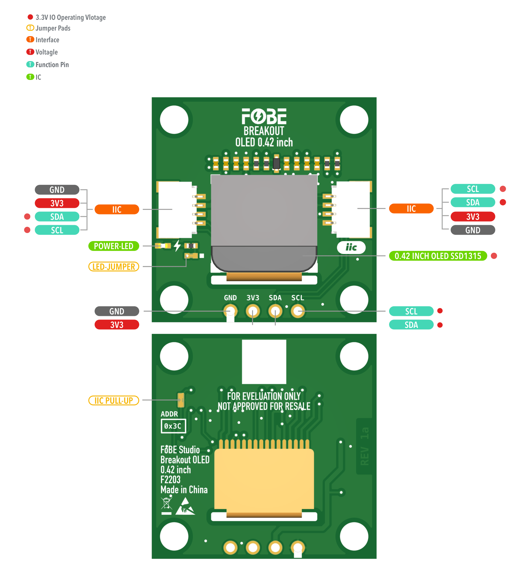
Hardware diagram
The following figure illustrates the FoBE Breakout OLED 0.42 inch hardware diagram.
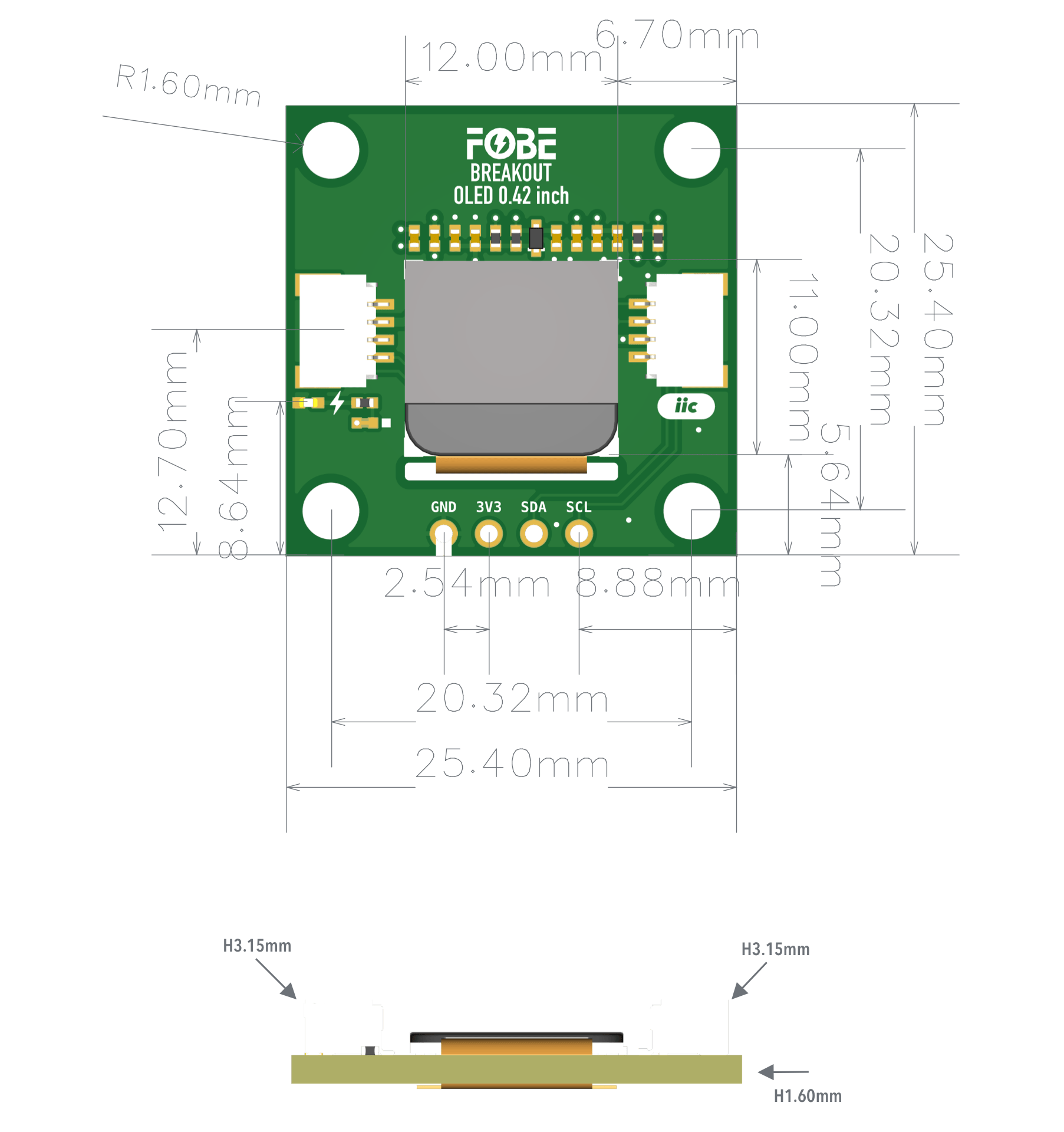
Mechanical dimensions
FoBE Breakout OLED 0.42 inch is a single-sided 25.4mm x 25.4mm (1" x 1") 1.6mm thick PCB with two SH1.0 4-pin connectors and a set of 4-pin 2.54mm header holes. Fixing by 4 x 1.6mm Screw holes.
Interfaces
The module provides dual 4-Pin JST SH1.0 connectors, compatible with STEMMA QT / Qwiic.
| 2.54mm 4-Pin | JST-SH1.0 | Features |
|---|---|---|
| GND | GND | Ground |
| 3V3 | 3V3 | Power supply, Only 3.3V |
| SDA | SDA | I2C-Data line |
| SCL | SCL | I2C-Clock line |
Advanced
Jumper
The module features two jumper pad:
| Interface | Description |
|---|---|
| LED-JUMPER | Disconnect this jumper to turn off the power LED for further power saving |
| IIC PULL-UP | Disconnect this jumper to disable I2C pull-up resistors if external pull-ups are used |
Programming
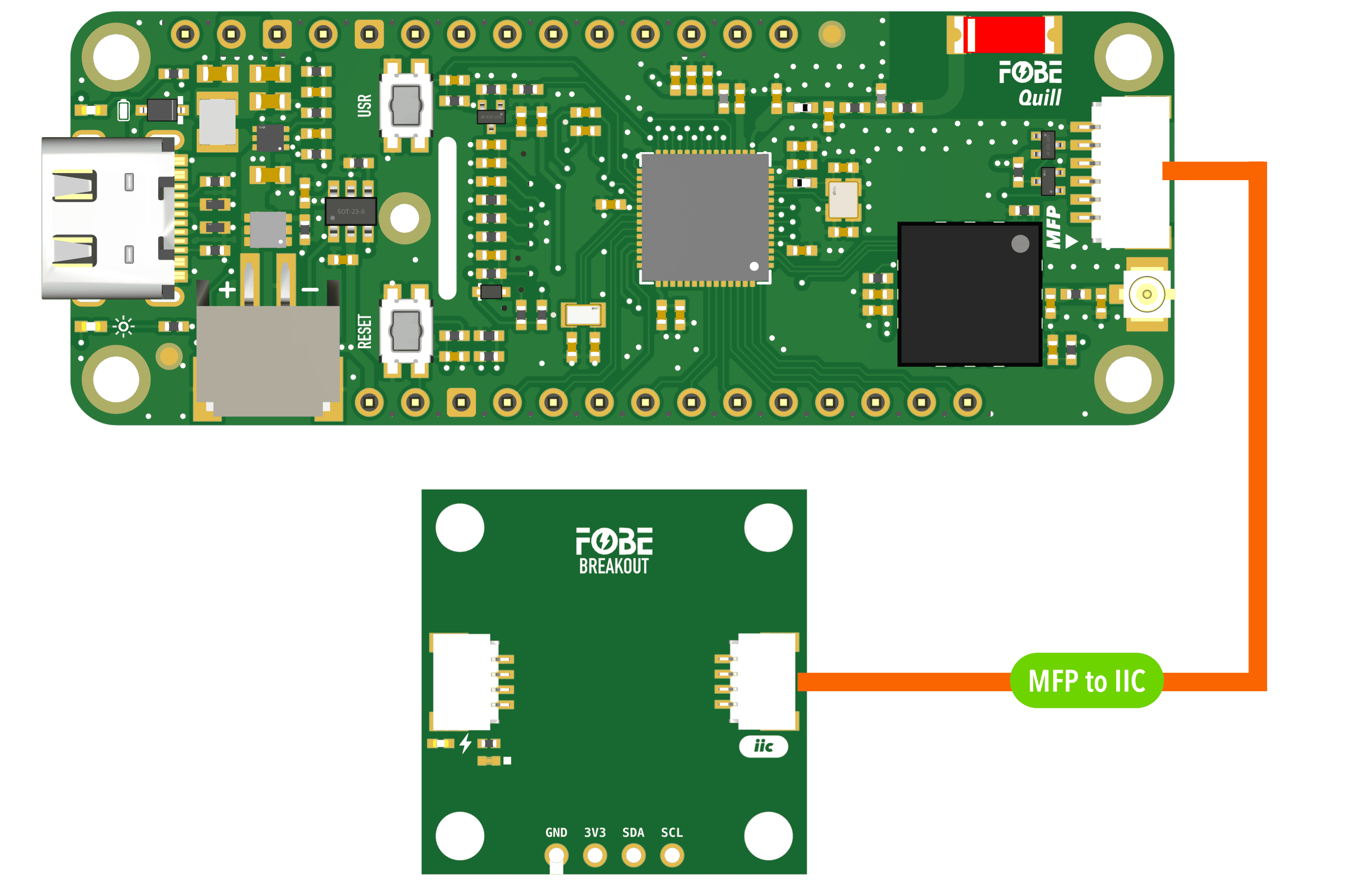
Running with FoBE Quill ESP32S3 Mesh
Let's get started with the FoBE Quill ESP32S3 Mesh using the MFP interface.
- Connect the FoBE Breakout OLED 0.42 inch to the FoBE Quill ESP32S3 Mesh using the MFP interface.
-
Create a sketch or PlatformIO project, or follow the FoBE Quill ESP32S3 Programming Guide for pre-configuration.
-
Install the necessary library in your project:
adafruit/Adafruit SSD1306@^2.5.15
adafruit/Adafruit GFX Library@^1.12.1
- Copy the following code into your sketch or PlatformIO project:
#include <Adafruit_GFX.h>
#include <Adafruit_SSD1306.h>

// Pin definitions
#define I2C_ADDRESS 0x3C        // I2C address for SSD1315 OLED
#define I2C_SDA_PIN PIN_MFP3    // SDA pin for I2C
#define I2C_SCL_PIN PIN_MFP4    // SCL pin for I2C
#define PERI_EN_PIN PIN_PERI_EN // Peripheral enable pin

// Display configuration for SSD1315 72x40 OLED
#define SCREEN_WIDTH 128        // Controller buffer width
#define SCREEN_HEIGHT 64        // Controller buffer height
#define DISPLAY_WIDTH 72        // Actual visible display width
#define DISPLAY_HEIGHT 40       // Actual visible display height
#define X_OFFSET 28            // Horizontal centering offset: (128-72)/2
#define Y_OFFSET 24            // Vertical centering offset: (64-40)/2 + 12
#define OLED_RESET -1          // Reset pin (not used)

TwoWire iic = TwoWire(1);
Adafruit_SSD1306 display(SCREEN_WIDTH, SCREEN_HEIGHT, &iic, OLED_RESET);

// Forward declaration
void showTestPattern();

void setup()
{
  // Initialize serial communication
  Serial.begin(115200);
  Serial.println("SSD1315 OLED Display Example");

  // Enable peripheral power
  if (PERI_EN_PIN >= 0)
  {
    pinMode(PERI_EN_PIN, OUTPUT);
    digitalWrite(PERI_EN_PIN, HIGH);
    Serial.println("Peripheral power enabled");
  }

  // Initialize I2C
  iic.begin(I2C_SDA_PIN, I2C_SCL_PIN);
  delay(200);

  // Initialize SSD1315 display
  Serial.println("Initializing SSD1315 display...");
  if (!display.begin(SSD1306_SWITCHCAPVCC, I2C_ADDRESS))
  {
    Serial.println("SSD1315 initialization failed, trying alternative...");
    if (!display.begin(SSD1306_EXTERNALVCC, I2C_ADDRESS))
    {
      Serial.println("SSD1315 initialization failed completely");
      for (;;); // Stop execution
    }
  }
  Serial.println("SSD1315 display initialized successfully");

  // Configure SSD1315 for 72x40 display
  display.clearDisplay();
  display.setTextWrap(false);

  // SSD1315-specific configuration
  display.ssd1306_command(SSD1306_SETDISPLAYOFFSET);
  display.ssd1306_command(0x00);                       // No hardware offset
  display.ssd1306_command(SSD1306_SETSTARTLINE | 0x0); // Start line 0
  display.ssd1306_command(SSD1306_SEGREMAP | 0x1);     // Column address remapping
  display.ssd1306_command(SSD1306_COMSCANDEC);         // COM scan direction
  display.ssd1306_command(SSD1306_SETCOMPINS);
  display.ssd1306_command(0x12);                       // COM pins configuration for 72x40
  display.ssd1306_command(SSD1306_SETCONTRAST);
  display.ssd1306_command(0x8F);                       // Set contrast
  display.ssd1306_command(SSD1306_MEMORYMODE);
  display.ssd1306_command(0x00);                       // Horizontal addressing mode

  // Display test pattern
  showTestPattern();
}

void showTestPattern()
{
  display.clearDisplay();

  // Draw border for the visible display area
  display.drawRect(X_OFFSET, Y_OFFSET, DISPLAY_WIDTH, DISPLAY_HEIGHT, SSD1306_WHITE);

  // Draw corner markers to verify orientation
  display.drawPixel(X_OFFSET + 1, Y_OFFSET + 1, SSD1306_WHITE);           // Top-left
  display.drawPixel(X_OFFSET + DISPLAY_WIDTH - 2, Y_OFFSET + 1, SSD1306_WHITE);    // Top-right
  display.drawPixel(X_OFFSET + 1, Y_OFFSET + DISPLAY_HEIGHT - 2, SSD1306_WHITE);  // Bottom-left
  display.drawPixel(X_OFFSET + DISPLAY_WIDTH - 2, Y_OFFSET + DISPLAY_HEIGHT - 2, SSD1306_WHITE); // Bottom-right

  // Add corner labels
  display.setTextSize(1);
  display.setTextColor(SSD1306_WHITE);
  display.setCursor(X_OFFSET + 2, Y_OFFSET + 2);
  display.print("TL");
  display.setCursor(X_OFFSET + 56, Y_OFFSET + 2);
  display.print("TR");
  display.setCursor(X_OFFSET + 2, Y_OFFSET + 30);
  display.print("BL");
  display.setCursor(X_OFFSET + 56, Y_OFFSET + 30);
  display.print("BR");

  // Center text showing resolution
  display.setCursor(X_OFFSET + 20, Y_OFFSET + 16);
  display.print("72x40");

  display.display();
  Serial.println("Test pattern displayed successfully");
}

void loop()
{
  // Main loop - add your application code here
}
- Build and upload the project. You should see the text on display.