Quick Start
This guide introduces the FoBE Mesh Solar Power and how to use it.
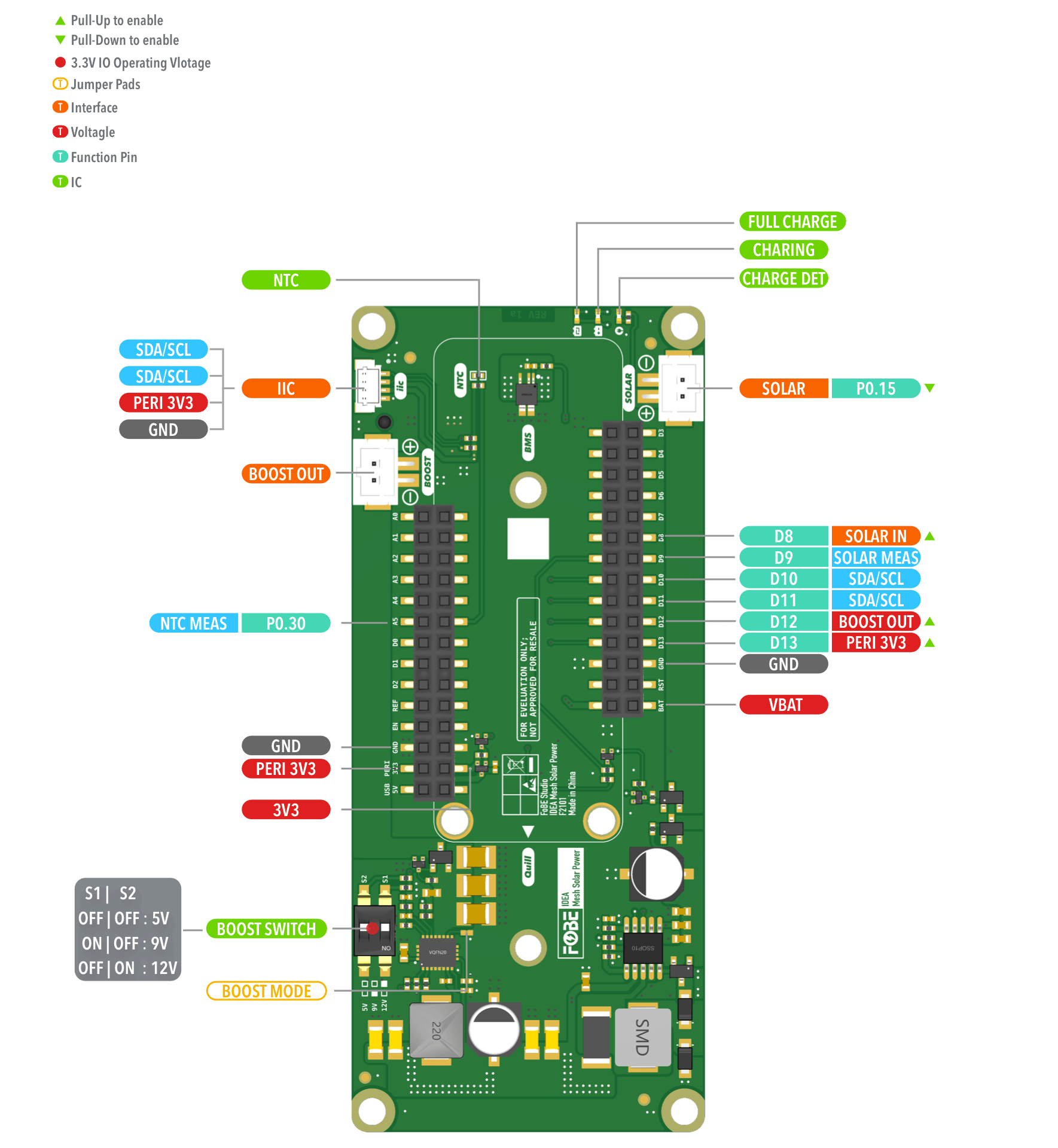
Hardware diagram
The following figure illustrates the FoBE Mesh Solar Power hardware diagram.
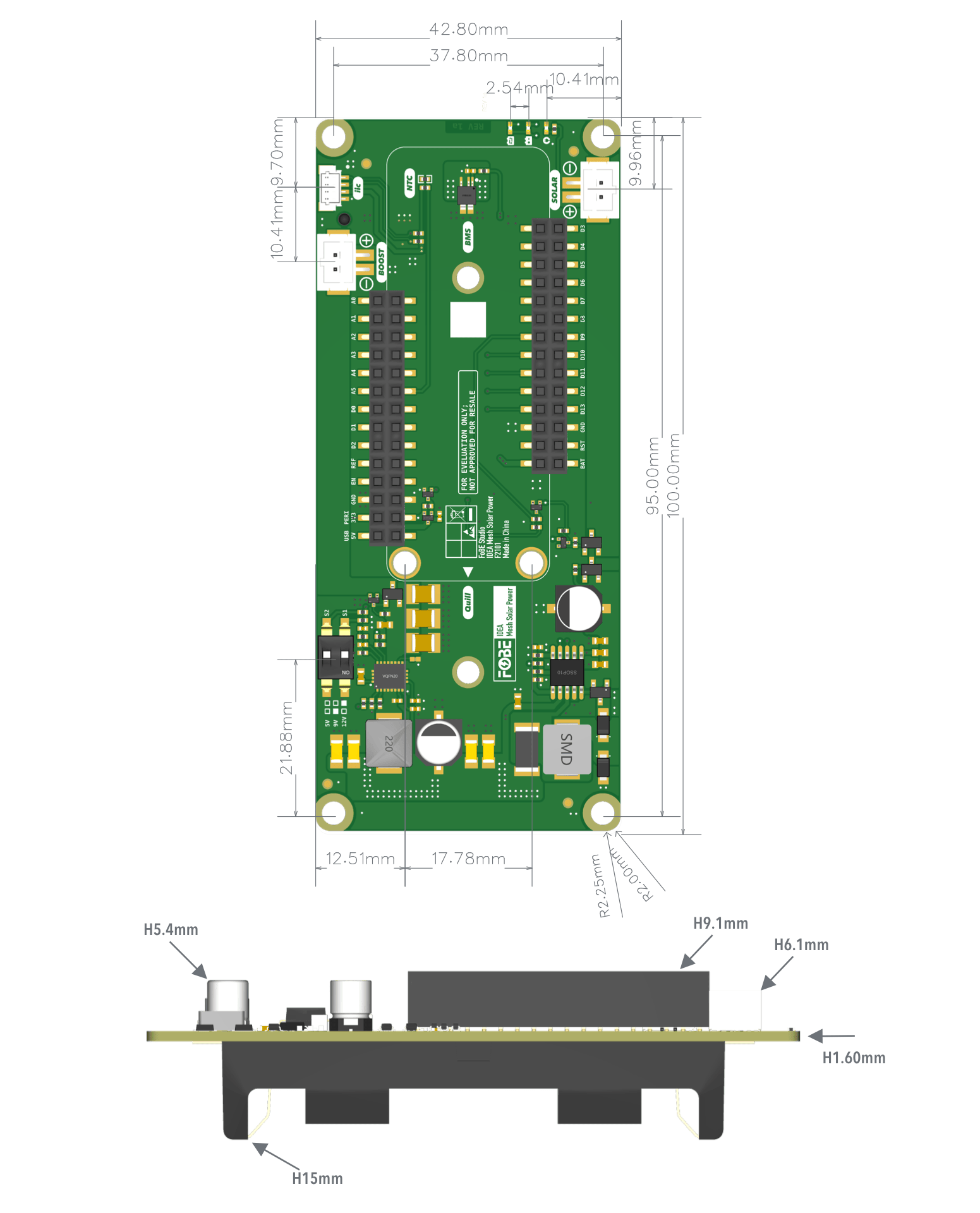
Mechanical dimensions
FoBE Mesh Solar Power is a PCB with dimensions of 100mm * 42.8mm, designed to be compatible with QUILL series devices, featuring two rows of double 14-pin female headers.
Power Output Configuration
The boost voltage output can be manually set using the 2-bit switch on the board. The S1/S2 switch configurations correspond to the following output voltages:
| S1 | S2 | Output Voltage |
|---|---|---|
| 0 | 0 | 5V |
| 1 | 0 | 9V |
| 1 | 1 | 12V |
Status Indicators
The board has three indicator LEDs:
- Solar Panel Input Voltage Indicator
- Solar Charging Indicator
- Battery Full Indicator
Peripheral Power
The external IIC power is provided by PERI-3V3, which is controlled by the Quill device via the D13 pin.
Onboard NTC
In addition to the battery protection chip, there is an onboard NTC measurement circuit(3380K, composed of PERI-3V3 and a 10k resistor) connected to pin A5. This NTC can be measured and monitored by the Quill device using the corresponding pin.
BOOST MODE Jumper
The board also has a reserved solder jumper: BOOST MODE. If soldered resistor, the boost converter operates in PWM mode; otherwise, it operates in PFM mode.
In moderate to heavy load condition, the device works in pulse width modulation (PWM) mode. In light load condition, the device has two operation modes selected by the MODE pin. One is the pulse frequency modulation (PFM) mode to improve the efficiency and another one is forced PWM mode to avoid application problems caused by low switching frequency. The switching frequency in PWM mode is adjustable, ranging from 200 kHz to 2.2 MHz by an external resistor.