Getting Started with FoBE Breakout GP8403
Introduction
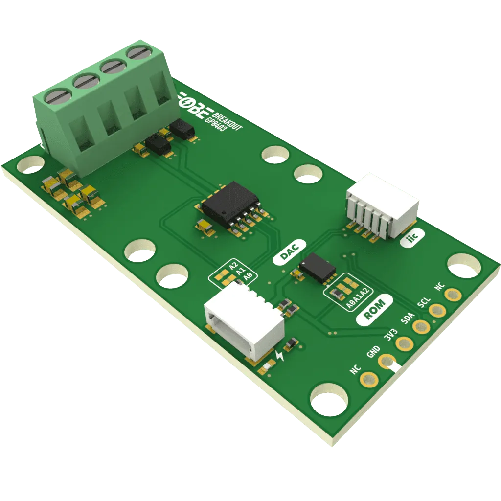
The FoBE Breakout GP8403 integrates the Linearin-GP8403 I2C to dual-channel voltage DAC converter and the ST- M24C64 EEPROM for calibration data storage. The module converts 12-bit digital values (0x000-0xFFF) to precise 0-5V or 0-10V analog voltage output with excellent linearity and accuracy. Multiple connectivity options are provided for easy integration into various applications.
Applications
- General signal conversion and conditioning
- Motor speed regulation and LED dimming control
- Inverter and power supply control systems
- Industrial analog signal isolation and processing
Key Features
-
GP8403
- Dual-channel 12-bit DAC resolution (0x000-0xFFF input range)
- Selectable output ranges: 0-5V or 0-10V per channel
- Excellent output voltage accuracy: < 0.5% (0.1% with calibration)
- Outstanding voltage linearity: 0.1%
- Output short circuit protection with automatic recovery
- I²C interface with programmable address
- Input I²C signal high level: 2.7V to 5.5V
- Power supply voltage: 9V to 36V
- Low power consumption: < 5mA
- Fast startup time: < 2ms
- Wide operating temperature: -40°C to +85°C
-
M24C64 EEPROM
- 64Kbit (8KB) data storage capacity
- 32-byte page size for efficient writing
- Write protection for entire memory array
- Enhanced ESD/Latch-Up protection
- More than 4 million write cycles endurance
- More than 200-years data retention
-
Connectivity
- MFP-IIC interface (JST-SH1.0 4-Pin)
- 6 x 2.54mm Pin Header
- 4 x 3.81mm Screw Terminal Block
Hardware diagram
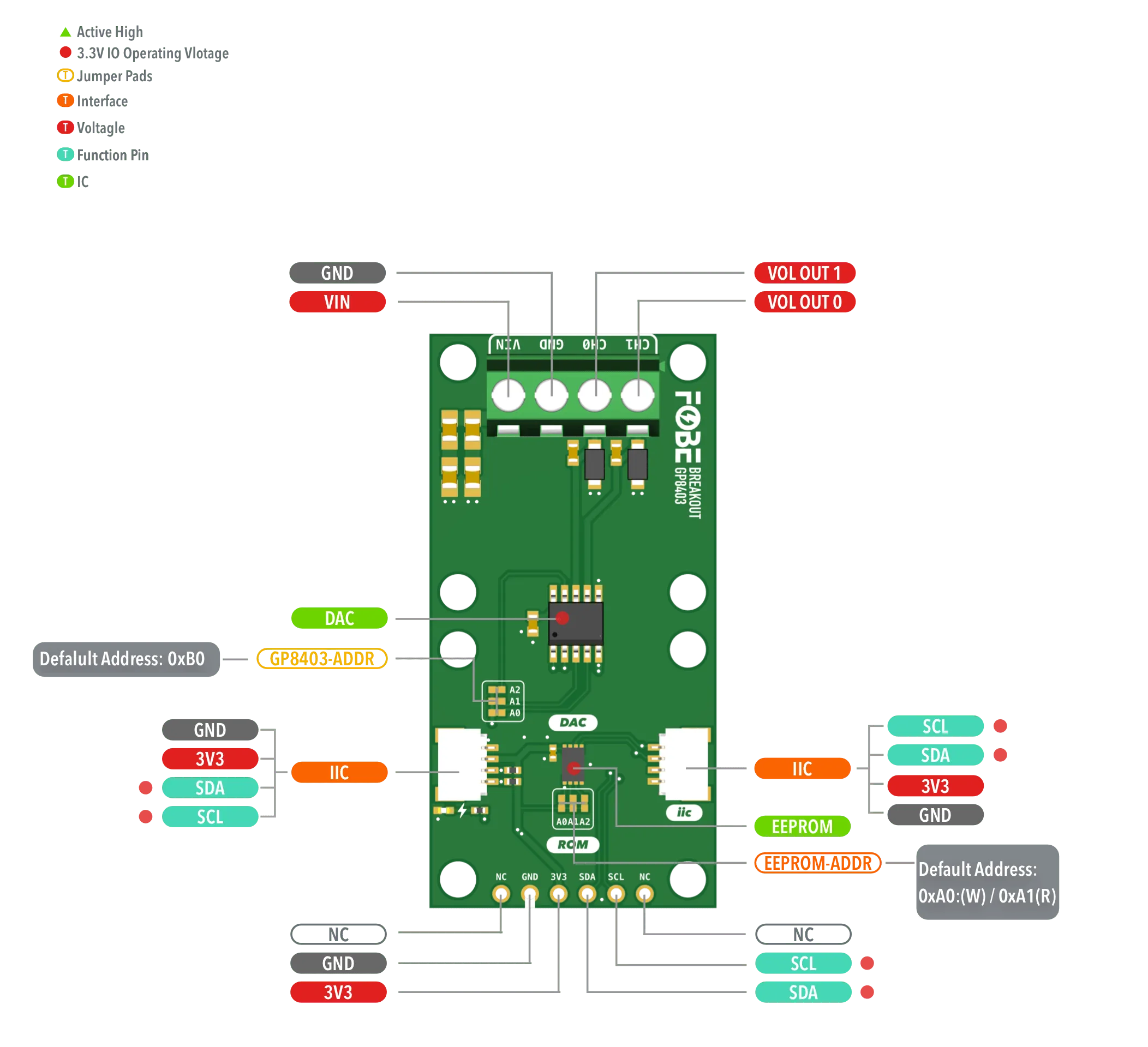
The following figure illustrates the FoBE Breakout GP8403 hardware diagram.
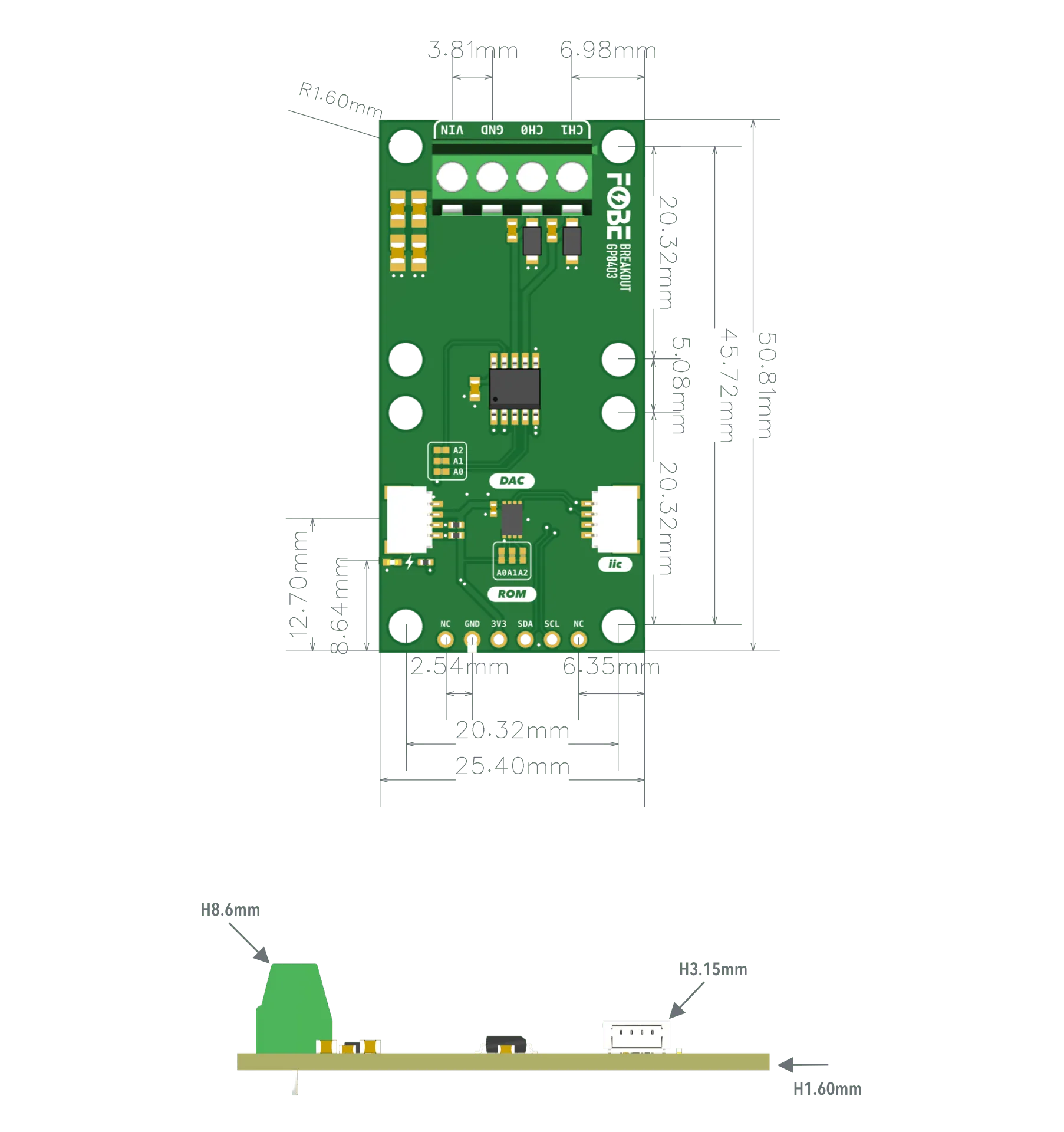
Mechanical dimensions
FoBE Breakout GP8403 is a single-sided 25.4mm x 50.8mm (1" x 2") 1.6mm thick PCB with two SH1.0 4-pin connectors, a set of 6-pin 2.54mm header holes, and 4 x 3.81mm screw terminal blocks for power and dual output. Fixing by 4 x 1.6mm Screw holes.
Interfaces
The module provides dual 4-Pin JST SH1.0 connectors, compatible with STEMMA QT / Qwiic.
| 2.54mm 6-Pin | JST-SH1.0 | Features |
|---|---|---|
| NC | — | Not connected |
| GND | GND | Ground |
| 3V3 | 3V3 | Power supply, Only 3.3V |
| SDA | SDA | I2C-Data line |
| SCL | SCL | I2C-Clock line |
| NC | — | Not connected |
Output Terminal Block
| 3.81mm Terminal | Features |
|---|---|
| VIN | Power supply: 9V to 36V |
| GND | Ground |
| CH1 | Channel 1 voltage output: 0-5V/0-10V |
| CH0 | Channel 0 voltage output: 0-5V/0-10V |
Advanced
Address Selection
GP8403 I2C Address
The GP8403 I²C address can be configured using solder pads A0-A2:
| A2 | A1 | A0 | I²C Address |
|---|---|---|---|
| 0 | 0 | 0 | 0x58 (Default) |
| 0 | 0 | 1 | 0x59 |
| 0 | 1 | 0 | 0x5A |
| 0 | 1 | 1 | 0x5B |
| 1 | 0 | 0 | 0x5C |
| 1 | 0 | 1 | 0x5D |
| 1 | 1 | 0 | 0x5E |
| 1 | 1 | 1 | 0x5F |
EEPROM I2C Address
The M24C64 EEPROM I²C address can be configured using solder pads A0-A2:
| A2 | A1 | A0 | I²C Address |
|---|---|---|---|
| 0 | 0 | 0 | 0x50 (Default) |
| 0 | 0 | 1 | 0x51 |
| 0 | 1 | 0 | 0x52 |
| 0 | 1 | 1 | 0x53 |
| 1 | 0 | 0 | 0x54 |
| 1 | 0 | 1 | 0x55 |
| 1 | 1 | 0 | 0x56 |
| 1 | 1 | 1 | 0x57 |
Programming
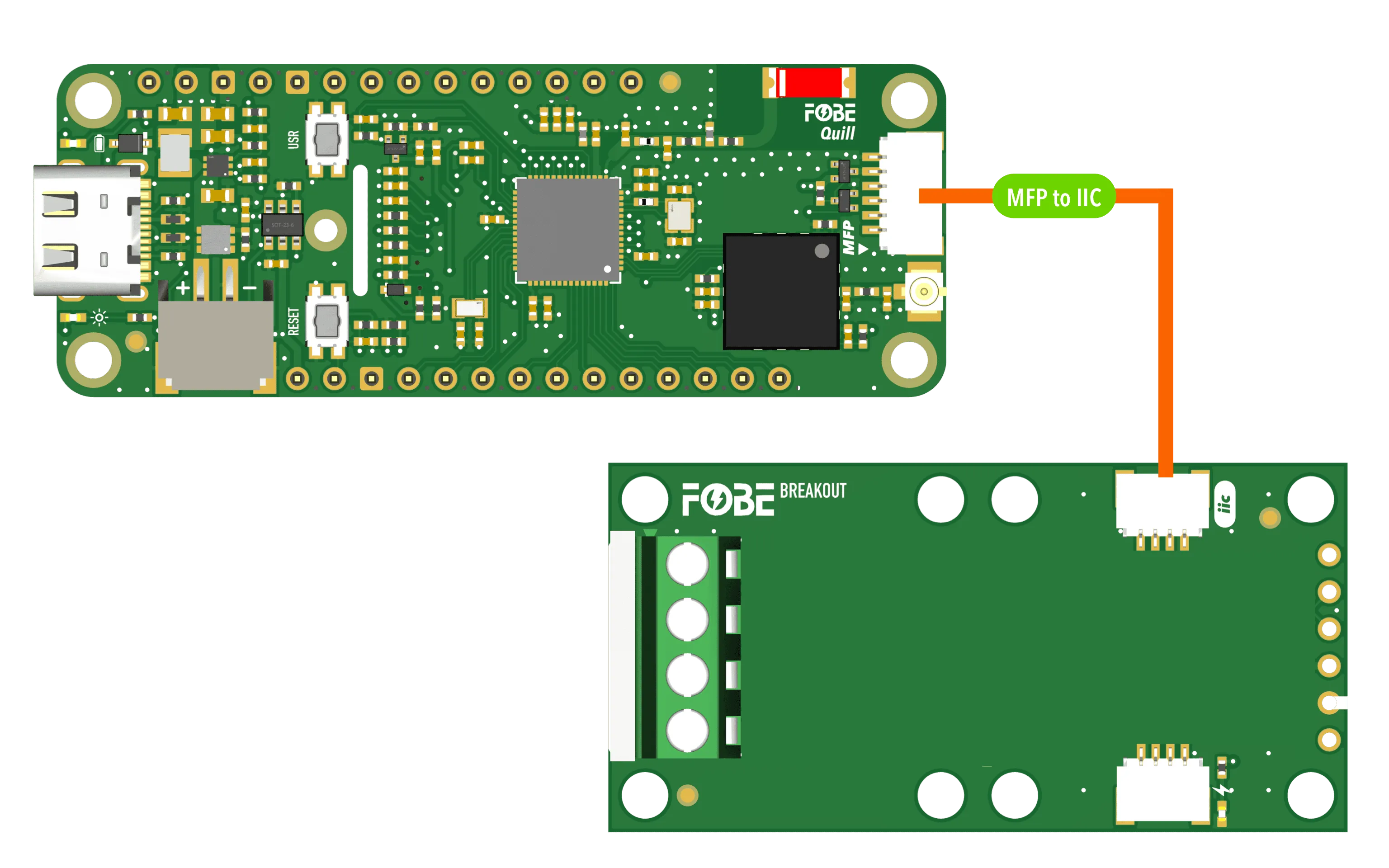
Running with FoBE Quill ESP32S3 Mesh
Let's get started with the FoBE Quill ESP32S3 Mesh using the MFP interface.
- Connect the FoBE Breakout GP8403 to the FoBE Quill ESP32S3 Mesh using the MFP interface.
-
Create a sketch or PlatformIO project, or follow the FoBE Quill ESP32S3 Programming Guide for pre-configuration.
-
Copy the following code into your sketch or PlatformIO project:
#include <Arduino.h>
#include <Wire.h>

#define GP8403_ADDR 0x58
#define GP8403_MODE_005V                0x00 // 0-5V output
#define GP8403_MODE_005_010V            0x10 // 0-5V and 0-10V output
#define GP8403_MODE_010_005V            0x01 // 0-10V and 0-5V output
#define GP8403_MODE_010V                0x11 // 0-10V output

#define GP8403_MODE_ADDRESS             0x01
#define GP8403_CHANNEL0_ADDRESS 0x02        // Channel 0 data register
#define GP8403_CHANNEL1_ADDRESS 0x04        // Channel 1 data register

#define IIC_SDA_PIN PIN_MFP3
#define IIC_SCL_PIN PIN_MFP4

bool setDACVoltage(uint8_t address, uint16_t vol_levl, uint8_t channel_reg) {
    uint8_t hibyte = ((vol_levl << 4) & 0xff00) >> 8;
    uint8_t lobyte = ((vol_levl << 4) & 0xff);
    vol_levl = lobyte << 8 | hibyte;
    Wire.beginTransmission(address);
    Wire.write((uint8_t)channel_reg);
    Wire.write((uint8_t)(vol_levl >> 8));
    Wire.write((uint8_t)(vol_levl & 0xFF));
    return (Wire.endTransmission() == 0);
}

void setup() {
    Serial.begin(115200);

    pinMode(PIN_PERI_EN, OUTPUT);
    digitalWrite(PIN_PERI_EN, HIGH);

    Wire.begin(IIC_SDA_PIN, IIC_SCL_PIN);

    Wire.beginTransmission(GP8403_ADDR);
    if (Wire.endTransmission() == 0) {
        Serial.println("GP8403 DAC found.");
    } else {
        Serial.println("GP8403 DAC not found. Check connections.");
        while (1) delay(1000);
    }

    Wire.beginTransmission(GP8403_ADDR);
    Wire.write((uint8_t)GP8403_MODE_ADDRESS);
    Wire.write((uint8_t)GP8403_MODE_005_010V);
    if(Wire.endTransmission() == 0){
        Serial.println("GP8403 mode set to 0-5V and 0-10V output.");
    } else {
        Serial.println("Failed to set GP8403 mode.");
        while (1) delay(1000);
    }

    setDACVoltage(GP8403_ADDR, 2047, GP8403_CHANNEL0_ADDRESS);
    Serial.println("Channel 0 set to approximately 2.5V.");

    setDACVoltage(GP8403_ADDR, 2047, GP8403_CHANNEL1_ADDRESS);
    Serial.println("Channel 1 set to approximately 5V.");
}

void loop() {
  delay(1000);
}
This example code sets Channel 0 to 3V and Channel 1 to 8V in 0-10V mode. Make sure to connect an appropriate power supply (9V-36V) to the VIN terminal and connect your measurement equipment to the CH0 and CH1 terminals.
# platformio.ini
[env:fobe_quill_esp32s3_mesh]
platform = FoBE Espressif 32
board = fobe_quill_esp32s3_mesh
framework = arduino
monitor_speed = 115200
monitor_raw = true
- Build and upload the project. You should measure 3V on channel 0 and 8V on channel 1 using a multimeter.
GP8403 DAC found.
GP8403 mode set to 0-5V and 0-10V output.
Channel 0 set to approximately 2.5V.
Channel 1 set to approximately 5V.
- If you want to use custom pins, you can change the
IIC_SDA_PINandIIC_SCL_PINdefinitions to your desired GPIO pins. - The GP8403 I²C address can be changed by soldering the appropriate address jumper pads on the board.
- Ensure proper 9V-36V power supply connection to VIN terminal for correct voltage output operation.
- Each channel can be independently configured for 0-5V or 0-10V output range.
Resources
[PDF] FoBE Breakout GP8403 Datasheet
[PDF] FoBE Breakout GP8403 Schematic