Getting Started with FoBE Breakout ADS1115
Introduction
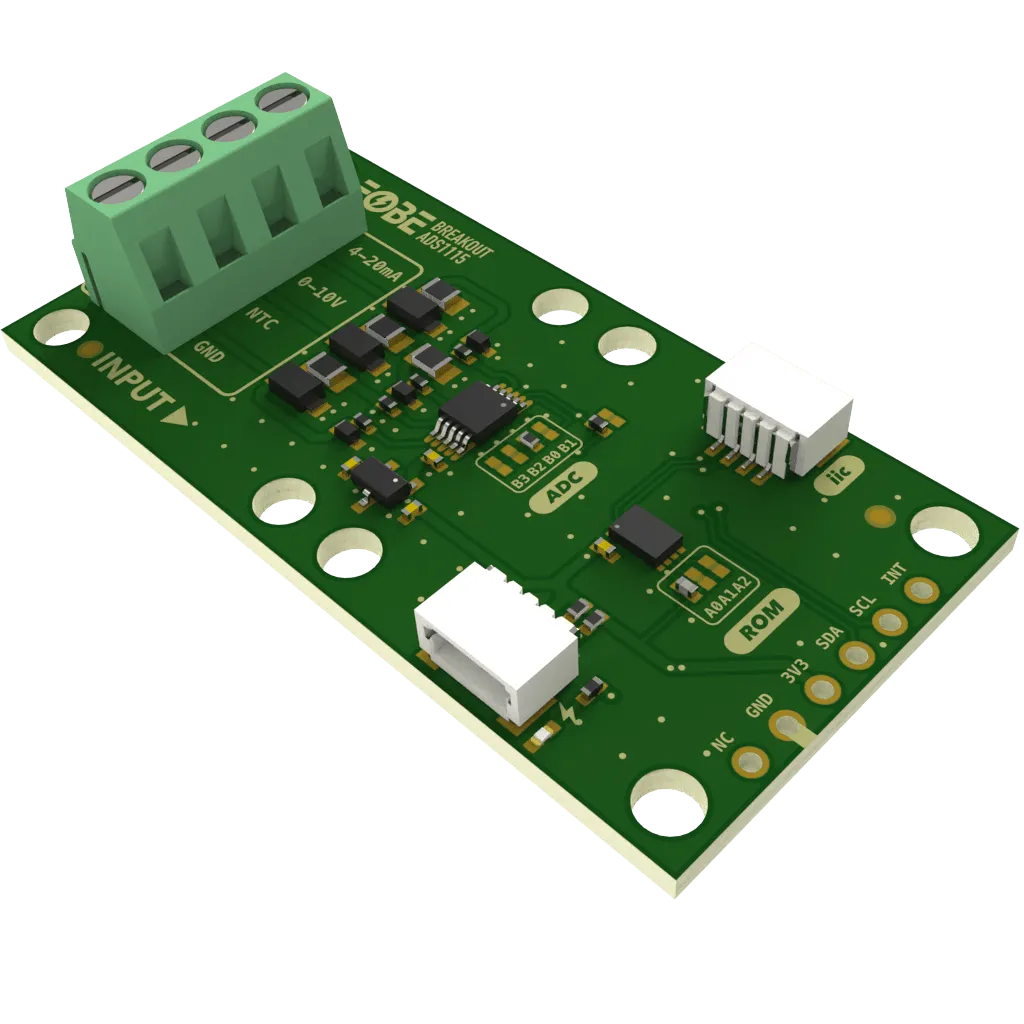
The FoBE Breakout ADS1115 integrates the TI-ADS1115 16-bit ADC with programmable gain amplifier and the EEPROM for calibration data storage. The module provides multiple measurement capabilities including 0-10V voltage measurement, 4-20mA current measurement, and NTC temperature measurement with built-in 2.5V reference. Multiple connectivity options are provided for easy integration into various applications.
Applications
- Portable instrumentation and measurement systems
- Battery monitoring and power management
- Temperature sensing and monitoring
- Factory automation and process controls
Key Features
-
ADS1115
- 16-bit high resolution analog-to-digital conversion
- 4 single-ended inputs or 2 differential inputs
- Programmable data rate: 8 SPS to 860 SPS
- Internal programmable gain amplifier (PGA): up to x16
- Internal low-drift voltage reference and oscillator
- I²C interface with programmable address
- Interrupt/ready pin for conversion completion
-
M24C64 EEPROM
- 64Kbit (8KB) data storage capacity
- I²C interface with programmable address
- Calibration data storage capability
-
Built-in Reference
- 2.5V precision voltage reference
- NTC measurement and ADC calibration support
-
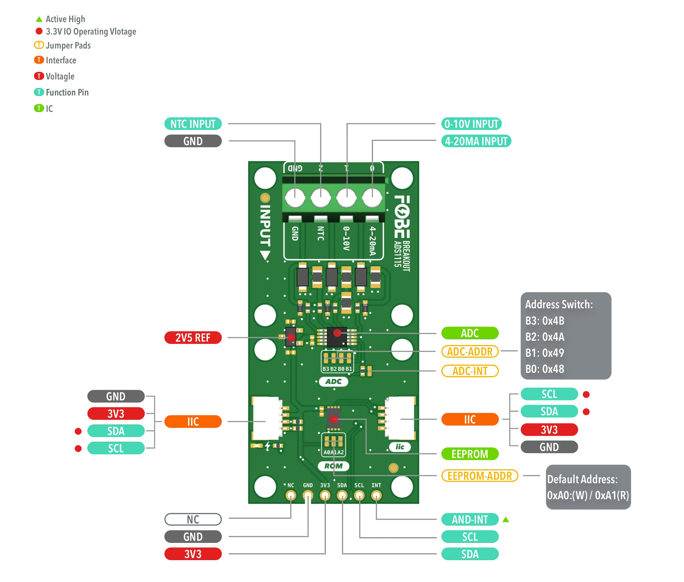
Connectivity
- MFP-IIC interface (JST-SH1.0 4-Pin)
- 6 x 2.54mm Pin Header
- 4 x 3.81mm Screw Terminal Block
Measure Channels
| Channel | Measurement Type | Description |
|---|---|---|
| 0 | 4-20mA current | Measured via 120Ω shunt resistor to ground |
| 1 | 0-10V voltage | Measured through voltage divider (10kΩ/39kΩ) |
| 2 | NTC temperature | Measured via voltage divider with 100kΩ resistor and 2.5V reference |
| 3 | NTC Reference | Connected to internal 2.5V voltage reference |
Hardware diagram
The following figure illustrates the FoBE Breakout ADS1115 hardware diagram.
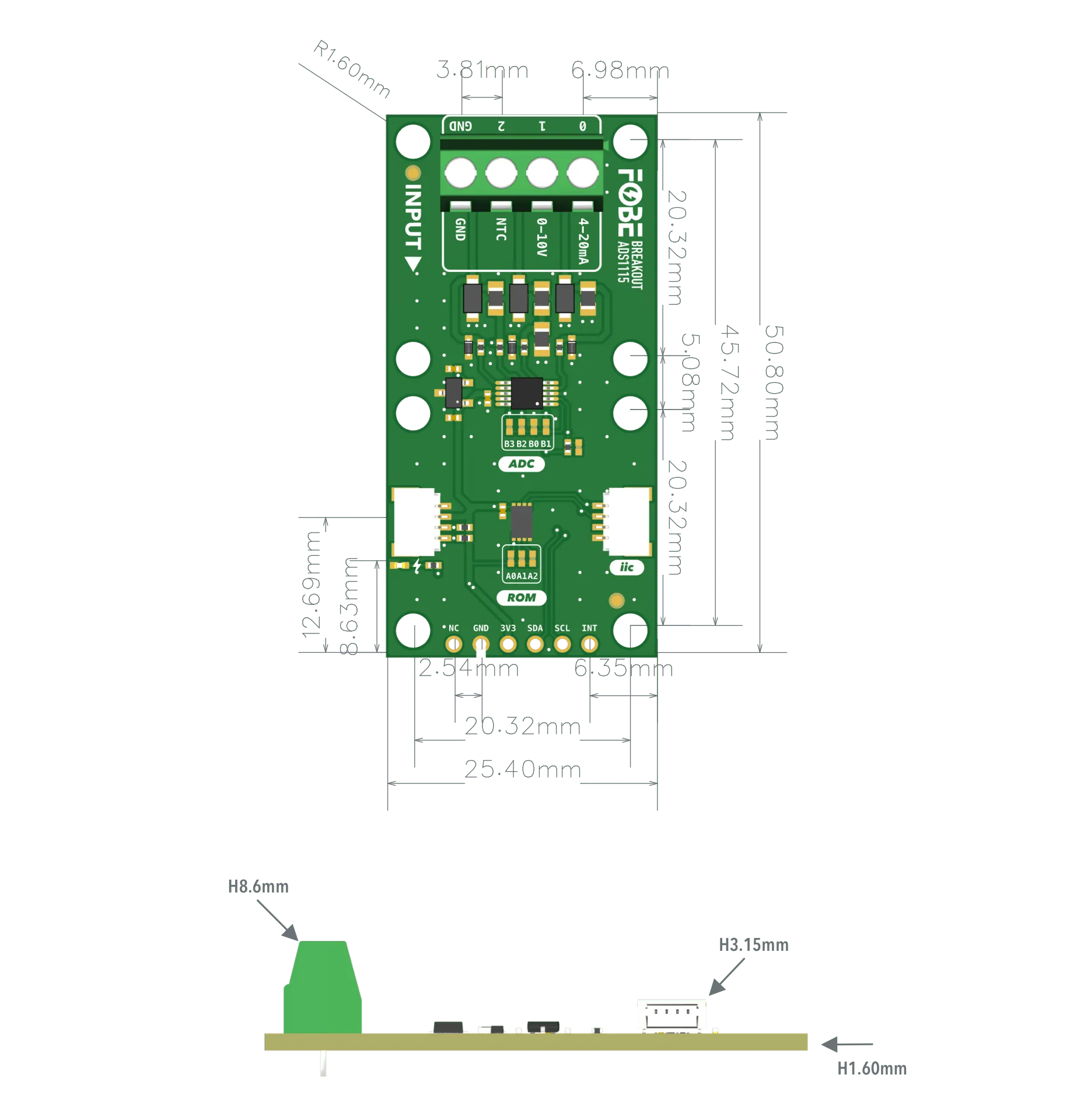
Mechanical dimensions
FoBE Breakout ADS1115 is a single-sided 25.4mm x 25.4mm (1" x 1") 1.6mm thick PCB with two SH1.0 4-pin connectors and a set of 6-pin 2.54mm header holes. Fixing by 4 x 1.6mm Screw holes.
Interfaces
The module provides dual 6-Pin JST SH1.0 connectors, compatible with STEMMA QT / Qwiic.
| 2.54mm 6-Pin | JST-SH1.0 | Features |
|---|---|---|
| NC | — | Not connected |
| GND | GND | Ground |
| 3V3 | 3V3 | Power supply, Only 3.3V |
| SDA | SDA | I2C-Data line |
| SCL | SCL | I2C-Clock line |
| INT | — | ADC conversion ready, Active Low |
Advanced
Address Selection
ADS1115 I2C Address
The ADS1115 I²C address can be configured using solder pads B0-B3:
| Pad | I²C Address |
|---|---|
| B0 | 0x48 (Default) |
| B1 | 0x49 |
| B2 | 0x4A |
| B3 | 0x4B |
EEPROM I2C Address
The M24C64 EEPROM I²C address can be configured using solder pads A0-A2:
| A2 | A1 | A0 | I²C Address |
|---|---|---|---|
| 0 | 0 | 0 | 0x50 (Default) |
| 0 | 0 | 1 | 0x51 |
| 0 | 1 | 0 | 0x52 |
| 0 | 1 | 1 | 0x53 |
| 1 | 0 | 0 | 0x54 |
| 1 | 0 | 1 | 0x55 |
| 1 | 1 | 0 | 0x56 |
| 1 | 1 | 1 | 0x57 |
Jumper
The module features one jumper pad:
| Interface | Description |
|---|---|
| ADC-INT | Connect this jumper to enable INT pin functionality for ADC conversion ready signal |
Measure Connections
| Channel | Type | Configuration |
|---|---|---|
| 0 | 4-20mA current | 120Ω shunt resistor to ground |
| 1 | 0-10V voltage | Voltage divider: 10kΩ (top) / 39kΩ (bottom) |
| 2 | NTC temperature | Voltage divider with 100kΩ resistor, 2.5V reference |
| 3 | Calibration | Internal 2.5V voltage reference |
Programming
Running with FoBE Quill ESP32S3 Mesh
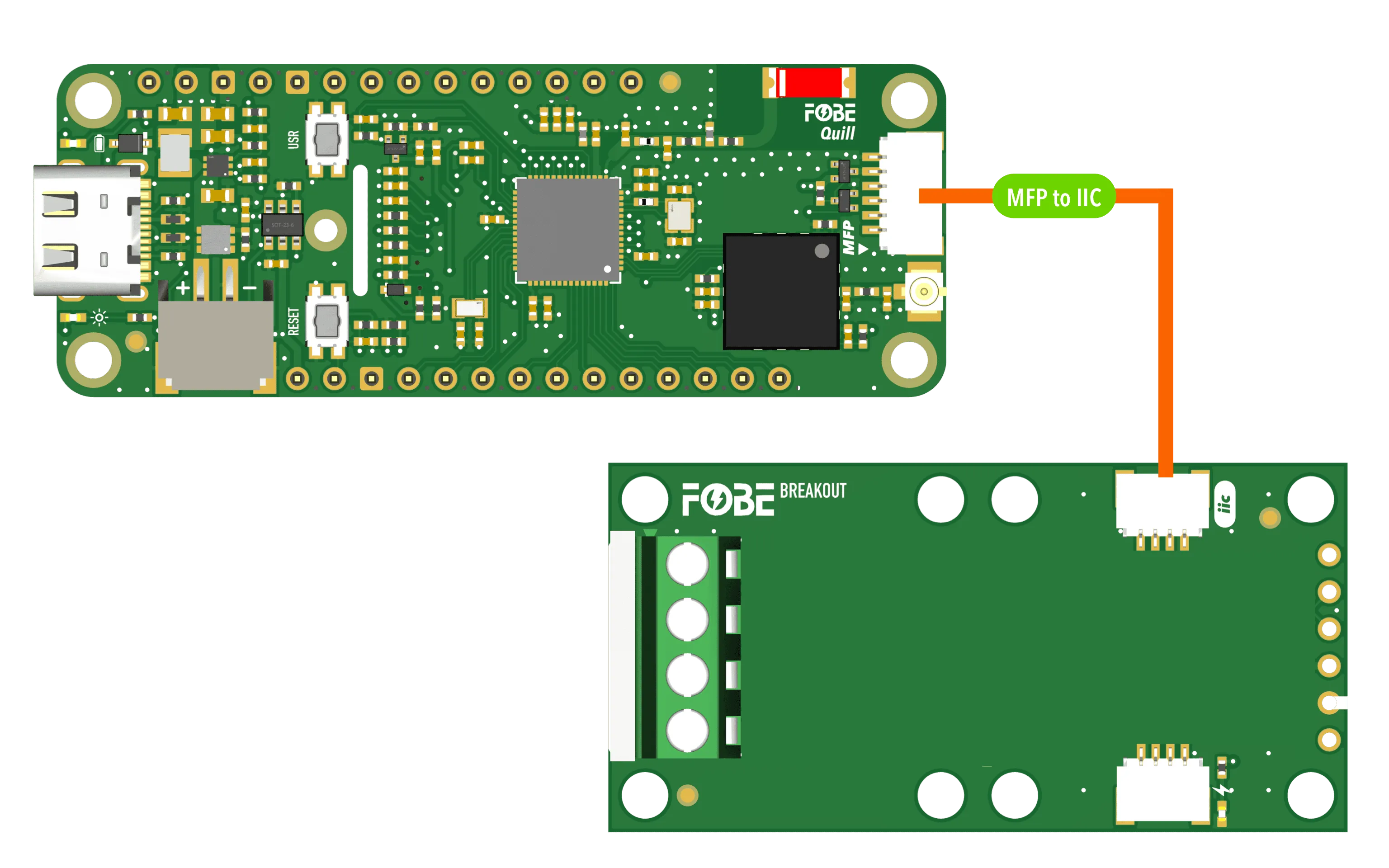
Let's get started with the FoBE Quill ESP32S3 Mesh using the MFP interface.
- Connect the FoBE Breakout ADS1115 to the FoBE Quill ESP32S3 Mesh using the MFP interface.
-
Create a sketch or PlatformIO project, or follow the FoBE Quill ESP32S3 Programming Guide for pre-configuration.
-
Install the necessary library in your project:
adafruit/Adafruit ADS1X15@^2.5.0
- Copy the following code into your sketch or PlatformIO project:
#include <Arduino.h>
#include <Wire.h>
#include <Adafruit_ADS1X15.h>

#define ADS1115_ADDR 0x48

#define IIC_SDA_PIN PIN_MFP3
#define IIC_SCL_PIN PIN_MFP4

Adafruit_ADS1115 ads;

void setup() {
  Serial.begin(115200); // Start serial communication at 9600 baud rate
  delay(3000);

  pinMode(PIN_PERI_EN, OUTPUT);
  digitalWrite(PIN_PERI_EN, HIGH);   // Enable peripheral power

  Wire.begin(IIC_SDA_PIN, IIC_SCL_PIN);

  if (!ads.begin(ADS1115_ADDR)) {
      Serial.println("Failed to initialize ADS.");
      while (1);
  }
}

void loop() {
  int16_t adc0, adc1, adc2, adc3;
  float volts0, volts1, volts2, volts3;

  adc0 = ads.readADC_SingleEnded(0);
  adc1 = ads.readADC_SingleEnded(1);
  adc2 = ads.readADC_SingleEnded(2);
  adc3 = ads.readADC_SingleEnded(3);

  volts0 = ads.computeVolts(adc0);
  volts1 = ads.computeVolts(adc1);
  volts2 = ads.computeVolts(adc2);
  volts3 = ads.computeVolts(adc3);

  Serial.println("> FoBE Breakout - ADS1115");
  Serial.print("\033[H\033[J"); // Clear terminal
  Serial.printf("\033[7m%-12s%-12s%-12s%-12s%-12s\033[0m",
              "Channel", "Value", "Voltage", "Result", "-");
  Serial.println();
  Serial.print("\033[0m");

  Serial.printf("%-12s%-12d%-12.6f%-12s%-12.6f", "AIN0", adc0, volts0, "4-20ma:", volts0/120*1000);
  Serial.println();

  Serial.printf("%-12s%-12d%-12.6f%-12s%-12.6f", "AIN1", adc0, volts1, "0-10V:", volts1 * (100000.0f + 39000.0f) / 39000.0f);
  Serial.println();

  const double Rp = 100000.0;  // 分压电阻
  const double R0 = 10000.0;  // 10k NTC
  const double T0 = 273.15 + 25.0; // 25℃
  const double Bx = 3950.0;
  const double Vref = 3.056250;     // 参考电压
  double Rt = volts2 / ((Vref - volts2) / Rp);
  double tempK = 1.0 / ( (1.0/T0) + (1.0/Bx) * log10(Rt / R0) );
  double tempC = tempK - 273.15;
  Serial.printf("%-12s%-12d%-12.6f%-12s%-12.6f", "AIN2", adc2, volts2, "NTC(˚C):", tempC);
  Serial.println();

  Serial.printf("%-12s%-12d%-12.6f%-12s%-12.6f", "AIN3", adc3, volts3, "REF-3V", volts3);

  delay(1000);
}
This example code shows basic ADC channel reading. Your terminal must support the output format to display the measurements correctly.
# platformio.ini
[env:fobe_quill_esp32s3_mesh]
platform = FoBE Espressif 32
board = fobe_quill_esp32s3_mesh
framework = arduino
lib_deps =
	adafruit/Adafruit ADS1X15@^2.5.0
monitor_speed = 115200
monitor_raw = true
- Build and upload the project. You should see the FoBE Breakout ADS1115 ADC channel data output in the serial monitor (raw mode).
Channel     Value       Voltage     Result      -
AIN0        0           0.000000    4-20ma:     0.000000
AIN1        0           0.002625    0-10V:      0.009356
AIN2        1136        0.213000    NTC(˚C):   27.849865
AIN3        16300       3.056250    REF-3V      3.056250
- If you want to use custom pins, you can change the
IIC_SDA_PINandIIC_SCL_PINdefinitions to your desired GPIO pins. - The ADS1115 is configured to use the default I²C address 0x48. You can change the address by soldering the appropriate jumper pads on the board.
Resources
[PDF] FoBE Breakout ADS1115 Datasheet
[PDF] FoBE Breakout ADS1115 Schematic